File:MicroChipAtomicTrap00.jpg

File originale (890 × 976 pixel, dimensione del file: 44 KB, tipo MIME: image/jpeg)
| Questo file e la sua pagina di descrizione (discussione · modifica) si trovano su Wikimedia Commons (?) |
| Descrizione |
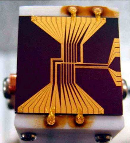
The first microchip atomic trap, designed at the Institute for Laser Science, Japan. The structure of wires is painted with gold at the insulator substrate. The main wire has Z-shape; the magnetic field allows the trapping of neutral atoms due to their magnetic momentum. The ship has sizes 2 x 2 cm. It was placed to the uniform magnetic field (source of this field is not shown in the figure); the traping is realized for so-called "atoms seeking for low magnetic field". The only atoms with positive spin-field energy were trapped. The miminim of the field is realized at the side of the chip, close to the central part of the z-electrode with electric current. This movement is limited by the edges of the "Z". Additional electrodes were designed to allow the play with the effective potential along this wire; the interaction with laser beams and reduction of the trapping potential allow the additional cooling of atoms (coling with vaporation), reaching the BEC. In the current design, the only one additional electrode is supplied with contacts. It was planned to use other electrodes to modify the potential in experiments with single-dimentional quantum mechanics. Actually, more advanced microchip atomic traps were manufactured instead. |
| Data | y.2003 |
| Fonte | private communication |
| Autore | Ken-Ichi Nakagawa |
| Licenza (Riusare questo file) |
copuleft directly from author |
| Altre versioni |
Up to my knowkedge, it is the best resolution image of the First Microship Atomic Trap, ever posted. lower resolution pics are available at
|

|
Il detentore del copyright di questo file permette a chiunque di utilizzarlo per qualsiasi scopo, a condizione che il detentore del copyright venga riconosciuto come tale. Sono consentiti la redistribuzione, la modifica, l'uso commerciale ed ogni altro utilizzo. |
|
|
Links
Cronologia del file
Fare clic su un gruppo data/ora per vedere il file come si presentava nel momento indicato.
| Data/Ora | Miniatura | Dimensioni | Utente | Commento | |
|---|---|---|---|---|---|
| attuale | 05:47, 12 set 2007 | | 890 × 976 (44 KB) | Domitori | {{Information |Description=The first microchip atomic trap, designed at Institute for Laser Science, Japan. The main wire has Z-shape; the magnetic field allows the trapping of neutral atoms due t |
Pagine che usano questo file
La seguente pagina usa questo file:
Utilizzo globale del file
Anche i seguenti wiki usano questo file:
- Usato nelle seguenti pagine di en.wikipedia.org:
- Usato nelle seguenti pagine di es.wikipedia.org:
- Usato nelle seguenti pagine di fa.wikipedia.org:
- Usato nelle seguenti pagine di fr.wikipedia.org:
- Usato nelle seguenti pagine di he.wikipedia.org:
- Usato nelle seguenti pagine di hr.wikipedia.org: