File:NE555 Bloc Diagram.svg

File originale (file in formato SVG, dimensioni nominali 723 × 524 pixel, dimensione del file: 32 KB)
| Questo file e la sua pagina di descrizione (discussione · modifica) si trovano su Wikimedia Commons (?) |
Dettagli
| Descrizione |
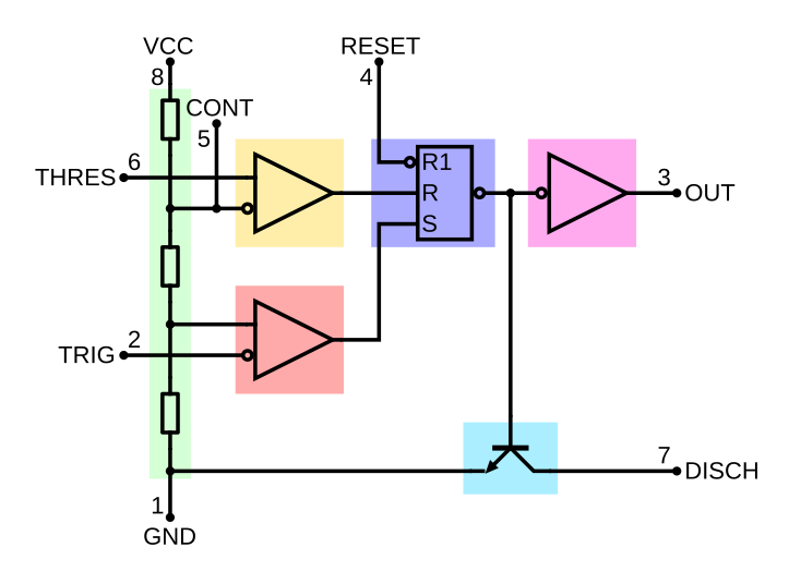
English: The NE555 contains 24 bipolar transistors, two diodes and 15 resistors that form six functional blocks:
Between the supply voltage VCC (+) and the ground GND (-) is a voltage divider consisting of three identical resistors which, when connected not from the outside, the two reference voltages ¹ / 3 VCC and ² / 3 VCC supplies. The latter is at the terminal pin Control Voltage available. The block diagram and schematic that area is highlighted in green. Two comparators are each connected to one of the reference voltages, while the other two inputs of which are fed directly to the terminals of trigger or threshold. The block diagram in yellow and orange. A flip-flop, deposited in the color purple, stores the state of the timer and is controlled by the two comparators. Via the reset terminal overrides the other two inputs, the flip-flop (and therefore the entire timer device) be reset at any time. At the output of flip-flop followed by an output stage with totem-pole output that can be loaded at the port output with up to 200 mA. Shown in the color pink. Parallel to the output stage of a transistor is connected, the collector is located on the discharge port. The transistor in the circuit diagram is a light blue background, always energized when the output is low level.Deutsch: Der NE555 enthält 24 Bipolartransistoren, zwei Dioden und 15 Widerstände, die zusammen sechs Funktionsblöcke bilden:
|
| Data | |
| Fonte | Opera propria |
| Autore | BlanchardJ |
| Altre versioni |
  |
Licenza
| Io, detentore del copyright su quest'opera, la rilascio nel pubblico dominio. Questa norma si applica in tutto il mondo. In alcuni paesi questo potrebbe non essere legalmente possibile. In tal caso: Garantisco a chiunque il diritto di utilizzare quest'opera per qualsiasi scopo, senza alcuna condizione, a meno che tali condizioni siano richieste dalla legge. |
Cronologia del file
Fare clic su un gruppo data/ora per vedere il file come si presentava nel momento indicato.
| Data/Ora | Miniatura | Dimensioni | Utente | Commento | |
|---|---|---|---|---|---|
| attuale | 21:54, 16 gen 2012 | | 723 × 524 (32 KB) | Wdwd | Colored function blocks (for circiut diagram) correct transistor symbol (without a circle, because it's inside the chip) |
| 01:27, 8 giu 2009 |  | 723 × 524 (40 KB) | Brighterorange | remove spurious red dot | |
| 22:22, 23 set 2007 |  | 723 × 524 (40 KB) | BlanchardJ | {{Information |Description=Bloc diagram of a 555 timer IC |Source=self-made |Date=September 23 2007 |Author=BlanchardJ |Permission= |other_versions= }} {{Created with Inkscape}} {{ElCompLib}} Category:555 timer IC |
Pagine che usano questo file
La seguente pagina usa questo file:
Utilizzo globale del file
Anche i seguenti wiki usano questo file:
- Usato nelle seguenti pagine di ar.wikipedia.org:
- Usato nelle seguenti pagine di beta.wikiversity.org:
- Usato nelle seguenti pagine di ca.wikipedia.org:
- Usato nelle seguenti pagine di cs.wikipedia.org:
- Usato nelle seguenti pagine di cs.wikibooks.org:
- Usato nelle seguenti pagine di de.wikipedia.org:
- Usato nelle seguenti pagine di en.wikipedia.org:
- Usato nelle seguenti pagine di es.wikipedia.org:
- Usato nelle seguenti pagine di et.wikipedia.org:
- Usato nelle seguenti pagine di fa.wikipedia.org:
- Usato nelle seguenti pagine di fi.wikipedia.org:
- Usato nelle seguenti pagine di fr.wikipedia.org:
- Usato nelle seguenti pagine di fr.wikiversity.org:
- Usato nelle seguenti pagine di he.wikipedia.org:
- Usato nelle seguenti pagine di hi.wikipedia.org:
- Usato nelle seguenti pagine di hu.wikipedia.org:
- Usato nelle seguenti pagine di id.wikipedia.org:
- Usato nelle seguenti pagine di ja.wikipedia.org:
- Usato nelle seguenti pagine di lt.wikipedia.org:
- Usato nelle seguenti pagine di no.wikipedia.org:
- Usato nelle seguenti pagine di pl.wikipedia.org:
- Usato nelle seguenti pagine di pt.wikipedia.org:
- Usato nelle seguenti pagine di ru.wikipedia.org:
- Usato nelle seguenti pagine di uk.wikipedia.org:
- Usato nelle seguenti pagine di vi.wikibooks.org:
- Usato nelle seguenti pagine di zh.wikipedia.org: